Magnetometer BMM350

BMM350 is a very small, high-performance, and low-current 16-bit 3-axis magnetometer. The digital sensor is ideally suited for a wide range of consumer applications such as AR/VR, head orientation, indoor navigation, magnetic compass, high-end gaming, and dead reckoning. The sensor is based on Bosch Sensortec’s proprietary TMR technology. The BMM350 magnetic sensor offers outstanding design flexibility, providing a single monolithic package solution.
- Unique field shock recovery feature
- High accuracy and ultra-low noise due to TMR technology
- Very low power consumption
| Order | |||
|---|---|---|---|
|
|
Out of Stock | 0 pieces | Not available |
|
|
Out of Stock | 0 pieces | Not available |
|
|
Out of Stock | 0 pieces | Not available |
|
|
Out of Stock | 0 pieces | Not available |
|
|
Out of Stock | 0 pieces | Not available |
Technical data
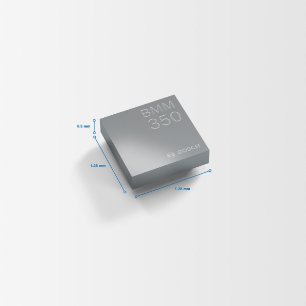
Package dimensions
1.28 x 1.28 x 0.5 mm³ wafer level chip scale package (WLCSP)
Operating range
-40 °C to 85 °C
Supply voltage
VDDIO: 1.72 V … 3.6 V
VDD: 1.72 V … 1.98 V
VDD: 1.72 V … 1.98 V
Typical output noise rms
3dB BW = ODR/2
3dB BW = ODR/2
± 190 nTrms (x,y axis) and
± 450 nT rms (z axis)
± 450 nT rms (z axis)
Sensitivity Temperature Drift (typ.)
± -0.010 %/K
Average typical current consumption
200 µA @ 100 Hz in normal mode
Magnetic field range, all axes
± 2000 µT
Zero-field offset drift after soldering (typ.)
± 25 µT
Sensitivity/gain error after soldering (typ.)
± 1 %
Interface
I2C and I3C
TCO error (typ.)
± 200 nT/K
Maximum sampling rate
400 Hz (normal mode)